
Product Center


ZB25VQ128
- Single 2.3V-3.6V supply
128 Mbit Serial Flash
- 128 M-bit/16M-byte/65,536 pages
- 256 bytes per programmable page
- Uniform 4K-byte Sectors, 32K/64K-byte Blocks
New Family of SpiFlash Memories
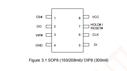
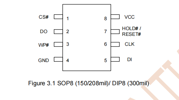
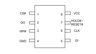
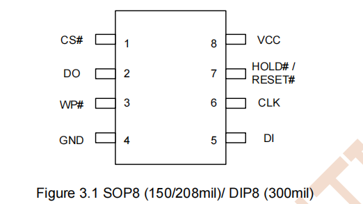
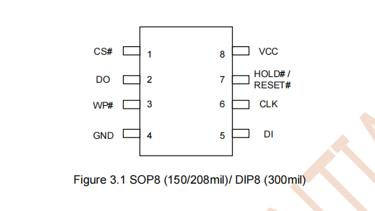
- Standard SPI: CLK, CS#, DI, DO, WP#, HOLD# / RESET#
- Dual SPI: CLK, CS#, DI, DO, WP#, HOLD# / RESET#
- Quad SPI: CLK, CS#, IO0, IO1, IO2, IO3
- QPI: CLK, CS#, IO0, IO1, IO2, IO3
- Software & Hardware Reset
- Auto-increment Read capability
The ZB25VQ128 of non-volatile flash memory device supports the standard Serial Peripheral Interface
(SPI). Traditional SPI single bit serial input and output (Single I/O or SIO) is supported as well as optional two
bit (Dual I/O or DIO) and four bit (quad I/O or QIO) serial protocols. This multiple width interface is called SPI
Multi-I/O or MIO.
The ZB25VQ128 support the standard Serial Peripheral Interface (SPI), Dual/Quad I/O SPI as well as
2-clocks instruction cycle Quad Peripheral Interface (QPI): Serial Clock, Chip Select, Serial Data I/O0 (DI),
I/O1 (DO), I/O2 (WP#), and I/O3 (HOLD# / RESET#). SPI clock frequencies of up to 104MHz are supported
allowing equivalent clock rates of 208MHz (104MHz x 2) for Dual I/O and 416MHz (104MHz x 4) for Quad I/O
when using the Fast Read Dual/Quad I/O and QPI instructions. These transfer rates can outperform standard
Asynchronous 8 and 16-bit Parallel Flash memories. The Continuous Read Mode allows for efficient memory
access with as few as 8-clocks of instruction-overhead to read a 24-bit address, allowing true XIP (execute in
place) operation.
A Hold pin, Write Protect pin and programmable write protection, with top or bottom array control, provide
further control flexibility. Additionally, the device supports JEDEC standard manufacturer and device ID and
SFDP Register, a 64-bit Unique Serial Number and three 256-bytes Security Registers.
The ZB25VQ128 provides an ideal storage solution for systems with limited space, signal connections,
and power. These memories' flexibility and performance is better than ordinary serial flash devices. They are
ideal for code shadowing to RAM, executing code directly (XIP), and storing reprogrammable data.
FEATURES
Low power supply operation
- Single 2.3V-3.6V supply
128 Mbit Serial Flash
- 128 M-bit/16M-byte/65,536 pages
- 256 bytes per programmable page
- Uniform 4K-byte Sectors, 32K/64K-byte Blocks
New Family of SpiFlash Memories
- Standard SPI: CLK, CS#, DI, DO, WP#, HOLD# / RESET#
- Dual SPI: CLK, CS#, DI, DO, WP#, HOLD# / RESET#
- Quad SPI: CLK, CS#, IO0, IO1, IO2, IO3
- QPI: CLK, CS#, IO0, IO1, IO2, IO3
- Software & Hardware Reset
- Auto-increment Read capability
Temperature Ranges
- Industrial (-40°C to +85°C)
- Extended (-20°C to +85°C)
Low power consumption
- 9 mA typical active current
- 2 uA typical power down current
Efficient “Continuous Read” and QPI Mode
- Continuous Read with 8/16/32/64-Byte Wrap
- As few as 8 clocks to address memory
- Quad Peripheral Interface(QPI) reduces instruction overhead
Flexible Architecture with 4KB sectors
- Sector Erase (4K-bytes)
- Block Erase (32K/64K-bytes)
- Page Program up to 256 bytes
- More than 100K erase/program cycles
- More than 20-year data retention
Advanced Security Feature
- Software and Hardware Write-Protect
- Power Supply Lock-Down and OTP protection
- Top/Bottom, Complement array protection
- Individual Block/Sector array protection
- 64-Bit Unique ID for each device
- Discoverable parameters(SFDP) register
- 3X256-Bytes Security Registers with OTP locks
- Volatile & Non-volatile Status Register Bits
High performance program/erase speed
- Page program time: 500us typical
- Sector erase time: 35ms typical
- Block erase time: 250ms typical
- Chip erase time: 50s typical
Package Options
- SOP8 - 208mil
- VSOP8 - 208mil
- DFN8 (5*6*0.75mm)/(6*8*0.75mm)
- TFBGA24
- All Pb-free packages are RoHS compliant
相关推荐
-
ZB25VQ40/20
The ZB25VQ40/20 of non-volatile flash memory device supports the standard Serial Peripheral Interface (SPI). Traditional SPI single bit serial input and output (Single I/O or SIO) is supported as well as optional two bit (Dual I/O or DIO) and four bit (quad I/O) serial protocols. This multiple width interface is called SPI Multi-I/O or MIO. -
ZB25VQ80
The ZB25VQ80 of non-volatile flash memory device supports the standard Serial Peripheral Interface (SPI). Traditional SPI single bit serial input and output (Single I/O or SIO) is supported as well as optional two bit (Dual I/O or DIO) and four bit (quad I/O) serial protocols. This multiple width interface is called SPI Multi-I/O or MIO. -
ZB25VQ16
The ZB25VQ16 of non-volatile flash memory device supports the standard Serial Peripheral Interface (SPI). Traditional SPI single bit serial input and output (Single I/O or SIO) is supported as well as optional two bit (Dual I/O or DIO) and four bit (quad I/O) serial protocols. This multiple width interface is called SPI Multi-I/O or MIO. -
ZB25VQ32
The ZB25VQ32 of non-volatile flash memory device supports the standard Serial Peripheral Interface (SPI). Traditional SPI single bit serial input and output (Single I/O or SIO) is supported as well as optional two bit (Dual I/O or DIO) and four bit (quad I/O or QIO) serial protocols. This multiple width interface is called SPI Multi-I/O or MIO. -
ZB25VQ64
The ZB25VQ64 of non-volatile flash memory device supports the standard Serial Peripheral Interface (SPI). Traditional SPI single bit serial input and output (Single I/O or SIO) is supported as well as optional two bit (Dual I/O or DIO) and four bit (quad I/O or QIO) serial protocols. This multiple width interface is called SPI Multi-I/O or MIO.